- Products
- Air Compressors & Air Tools
- Climate Control
- Compaction Equipment
- Concrete Cutting Tools & Equipment
- Concrete and Masonry
- Demolition & Excavation
- Electrical & Mechanical
- Fasteners and Anchoring Adhesives
- Floor Protection
- Generators and Welders
- Hand Tools
- Heaters
- Janitorial and Office Supplies
- Jobsite Protection
- Ladders & Storage
- Lighting & Lighting Accessories
- Man Lifts
- Material Handling Equipment
- Power Tools
- Pressure Washers & Pumps
- Safety Gear
- Safety Products
- Saws
- Surface Preparation
- SEASONAL PRODUCTS
- Rentals
- Air Compressor and Air Tool Rentals
- Climate Control Rental
- Compaction Rentals
- Concrete Equipment Rentals
- Demolition & Excavation Equipment Rentals
- Concrete Floor Grinder Rentals
- General Construction Equipment Rentals
- Generator Rentals and Welder Rentals
- Heater Rentals
- Light Tower Rentals
- Man Lift Rentals in Massachusetts and Rhode Island
- Material Handling Equipment Rentals
- Pressure Washer & Pump Rentals
- Saw Rentals in New England
- SEASONAL PRODUCTS
- Products
- Air Compressors & Air Tools
- Climate Control
- Compaction Equipment
- Concrete Cutting Tools & Equipment
- Demolition & Excavation
- Electrical & Mechanical
- Floor Protection
- Generators and Welders
- Construction Heaters
- Construction Ladders, Staging, & Storage
- Construction Lighting
- Man Lifts
- Material Handling Equipment
- Industrial Janitorial and Office Supplies
- Pressure Washers & Pumps
- Construction Safety Products
- Construction Safety Gear
- Surface Preparation
- Building Protection
- Diesel Accessories
- Zero Emissions
- Rentals
- Air Compressor and Air Tool Rentals
- Climate Control Rental
- Compaction Rentals
- Concrete Equipment Rental
- Demolition & Excavation Equipment Rental
- General Construction Equipment Rental
- Generator Rentals and Welder Rentals
- Construction Heaters Rental
- Light Tower Rentals
- Man Lift Rentals
- Material Handling Equipment Rental
- Pressure Washer & Pump Rentals
- Saw Rentals in New England
- Concrete Floor Grinder Rentals
- Zero Emissions Rentals
- Repairs & Used
- Parts
- Blog
- Services
- Resources
- About Us
- Contact Us
Sales & Rental of Construction | Industrial Equipment & Supplies


How to Choose a Hybrid Inverter PCB in 2026?
Choosing the right Hybrid Inverter Pcb in 2026 requires more than comparing prices or copper thickness. The board sits at the center of a demanding energy system. It must manage battery storage, solar input, grid interaction, and changing loads without losing control. A poor decision may appear acceptable during factory testing, then fail after months of heat, vibration, and repeated power cycles.
Start with the inverter’s electrical profile. Check maximum voltage, continuous current, surge duration, switching frequency, and isolation requirements. The PCB layout should provide suitable creepage and clearance distances. It should also control electromagnetic interference around high-speed switching devices. Thermal design matters just as much. Large copper areas, thermal vias, airflow paths, and reliable heat-spreading materials can prevent local hot spots near MOSFETs and capacitors. Small details become expensive failures.
Material selection deserves equal attention. High-Tg laminates may support demanding thermal cycles, while controlled impedance can improve signal stability. However, premium materials cannot repair a weak layout. Ask manufacturers for traceability records, inspection results, aging data, and compliance documentation. Verify testing under realistic battery and grid conditions, not only ideal laboratory loads. Standards and certifications should match the target market and product design.
There is no universal best board.
An experienced team should review supplier capability, repair access, production consistency, and long-term component availability. Initial assumptions can be wrong, especially when a prototype performs well but lacks field endurance. For this reason, compare measured evidence with datasheets, inspect failure history, and leave room for design revision. The strongest Hybrid Inverter Pcb is not simply the most advanced option. It is the one that remains safe, stable, serviceable, and dependable throughout its expected operating life.
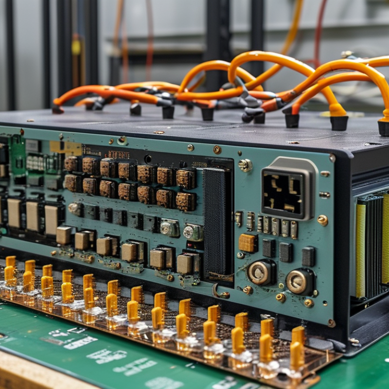
Table of Contents [Hide]
Define the Role and Requirements of a Hybrid Inverter PCB
How to Choose a Hybrid Inverter PCB in 2026?
A hybrid inverter PCB manages power between solar panels, batteries, loads, and the utility connection. Its role is more than switching current. It also controls charging, conversion, protection, communication, and fault responses. Define these functions before comparing board specifications. A 48 V battery system may need high-current copper paths, accurate voltage sensing, and controlled inrush protection. A grid-connected design requires isolation, reliable gate control, and carefully managed electromagnetic interference. Thermal performance matters too. Check heat around MOSFETs, transformers, connectors, and current sensors. Small hot spots can become expensive failures.
Tips: Write a requirement sheet first. Include input range, output power, switching frequency, operating temperature, cooling method, and expected service life. Ask for test evidence, not only impressive ratings. Review creepage, clearance, overcurrent protection, and communication interfaces. Examine whether the PCB supports firmware updates and clear fault reporting. These details often decide whether maintenance is simple or frustrating.
In practical design reviews, a high-rated PCB is not always the best choice. Its connectors may be weak, or its thermal design may rely on ideal airflow. That assumption deserves challenge. I would inspect waveforms under light and peak loads, then check temperature after repeated cycles. Efficiency should be measured across realistic battery voltages, not one convenient point. Leave room for uncertainty. Field conditions are rarely perfect, and a design that ignores dust, vibration, or aging may look excellent only on paper.

© Copyright - Pro Tool & Supply - Site by SVM E-Marketing Solutions - Sitemap
- Privacy policy